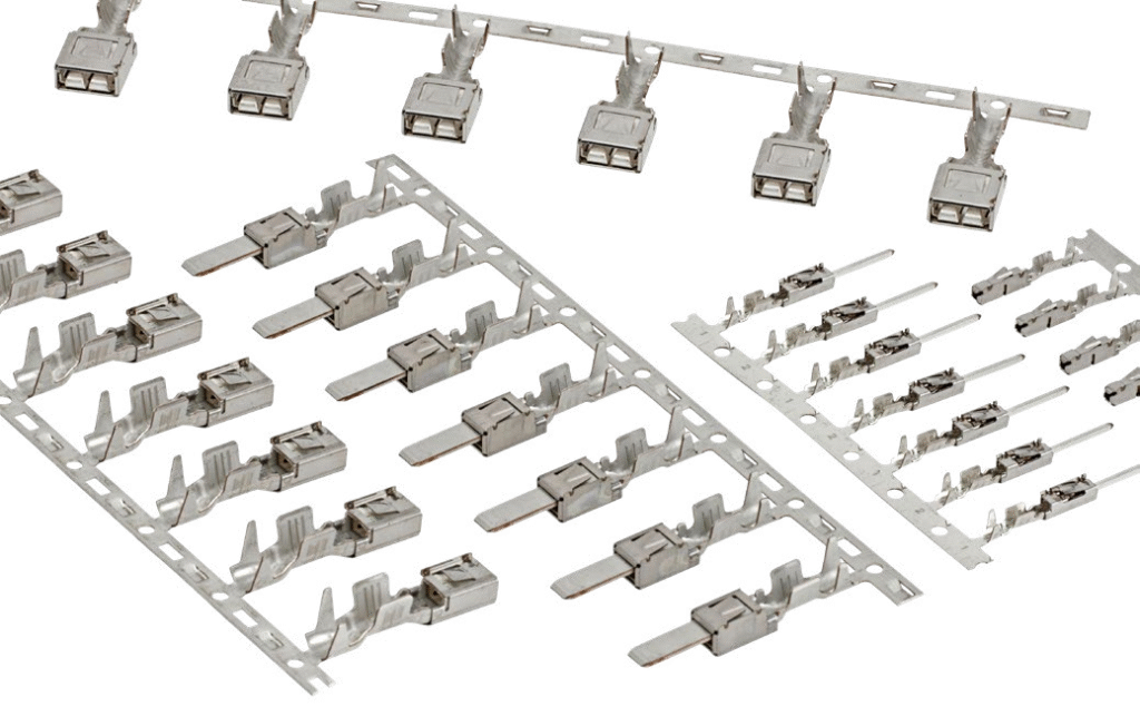
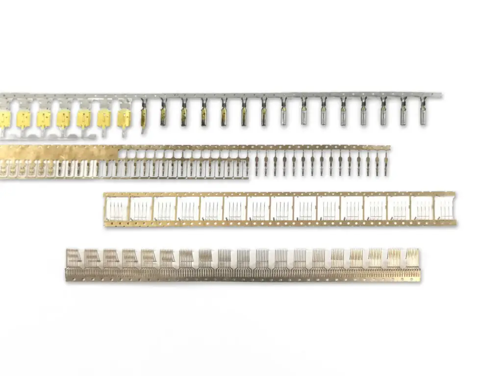
For manufacturers relying on precision stamping processes, chip/scraps jumping is more than just an annoyance—it’s a critical issue that threatens product quality, mold longevity, and production efficiency. When metal chips/scraps bounce or accumulate in die gaps during stamping, they can scratch workpiece surfaces, cause dimensional inaccuracies, damage cutting edges, and even lead to unplanned downtime for mold cleaning.
As a professional precision stamping die manufacturer with years of engineering experience, we’ve refined chip control solutions for diverse materials (steel, aluminum, copper, alloys) and stamping scenarios (fine blanking, high-speed stamping, micro-stamping). Below are 8 proven chip prevention methods tailored to precision dies, designed to eliminate chip-related headaches and elevate your production reliability.
1. Vacuum Suction Chip Control (Ideal for Fine, Light Chips)
How It Works
Integrate micro air channels (0.5–1.5mm diameter) into punch inserts, die cavities, or stripper plates, connected to a vacuum system. Negative pressure (-0.06~-0.09MPa) generated during stamping instantly sucks chips into a dedicated collection chamber, blocking bounce paths.
Key Advantages
- Zero chip residue on workpieces, critical for ultra-precision components (e.g., electronic connectors, sensor housings).
- Compatible with thin materials (0.1–1.0mm) and fine blanking processes.
- Equipped with 300–500 mesh filters to protect the vacuum pump from debris damage.
Ideal Applications
Precision stamping of thin-gauge metals (stainless steel, copper alloys) and micro-components where surface finish and dimensional accuracy are non-negotiable.
2. Magnetic Chip Adsorption (For Ferromagnetic Materials)
How It Works
Embed neodymium magnets (high magnetic strength, compact size) inside the die—typically near the die cutting edge, punch retainer, or stripper plate (1–2mm distance from the edge to avoid interfering with stamping action). Magnets attract iron/steel chips, preventing them from bouncing in the die.
Key Advantages
- Low maintenance: 搭配 scrapers for automatic chip removal after each stamping cycle.
- No airflow or pressure interference, suitable for stable precision stamping.
- Magnetic shielding (e.g., copper sleeves) optional to avoid affecting electronic components.
Ideal Applications
Stamping ferromagnetic materials (cold-rolled steel, spring steel) for automotive parts, hardware accessories, or industrial fasteners. Not recommended for non-magnetic materials like aluminum or plastic.
3. Chip Grooves + Guide Plates (Universal for Medium-Sized Chips)
How It Works
Design inclined chip grooves (15°–30° angle) on the die or stripper plate, paired with polished guide plates (HRC58–62 hardened steel, Ra≤0.8μm surface finish). Chips are guided by gravity and stamping force along the grooves to a collection bin, eliminating rebound.
Key Advantages
- Versatile: Works for medium-thickness materials (1.0–5.0mm) and general blanking processes.
- Prevent chip jamming: Groove width is 2–3mm larger than maximum chip size, with a depth ≥5mm.
- Non-intrusive design: Grooves avoid critical die components (locating pins, guide pillars).
Ideal Applications
General precision stamping (gear blanks, hardware fittings) and multi-station progressive dies where continuous chip discharge is required.
4. Combined Vacuum + Guide Grooves (For Complex Shapes)
How It Works
Combine the best of both worlds: add micro vacuum channels inside chip grooves to create negative pressure, guiding chips along the grooves while preventing bounce within the channel itself.
Key Advantages
- Solves chip accumulation in irregular die cavities (e.g., special-shaped holes, curved workpieces).
- Boosts chip evacuation efficiency by 30% compared to single guide grooves.
Ideal Applications
Complex precision stamping (custom automotive parts, medical device components) and multi-step forming processes.
5. Enhanced Elastic Pressure Plate (For High-Speed Stamping)
How It Works
Optimize the pressure plate’s design to increase clamping force by 10%–20% (matched to press tonnage to avoid material deformation). Tight clamping eliminates air turbulence between the material and die, reducing chip splash during material fracture.
Key Advantages
- Reduces chip generation at the source by minimizing material vibration.
- Uses polyurethane or nitrile rubber (Shore A 85–90) with micro-grooves (0.3–0.5mm width) for improved air release and chip retention.
- Nitrogen cylinder-driven pressure plates ensure uniform clamping force for high-speed stamping (≥300 strokes/min).
Ideal Applications
High-speed precision stamping of thin materials (e.g., smartphone frame parts, battery connectors) where production speed and consistency are priorities.
6. Cutting Edge Optimization (Source Chip Reduction)
How It Works
Redesign die cutting edges to alter material fracture behavior, reducing chip velocity and bounce angle— the most fundamental chip control solution.
Key Modifications
- Die edge: Adopt negative angles (-5°~-10°) to direct chips inward instead of outward.
- Punch edge: Add micro chamfers (R0.02–0.05mm) to prevent sharp, high-bounce chips from tearing.
- Clearance control: Maintain 5%–10% of material thickness (≤3% for ultra-precision stamping) to minimize chip size.
Key Advantages
- Improves both chip control and die life by reducing edge wear.
- No additional components required, cost-effective for long-term production.
Ideal Applications
All precision stamping processes, especially for medical device parts and micro-motor components requiring strict dimensional tolerance.
7. High-Pressure Air Blowing (For Automated Lines)
How It Works
Install micro air nozzles near the die cutting edge (45° angle, 3–5mm distance from the edge). Synchronized with the stamping cycle, dry compressed air (0.4–0.6MPa, moisture ≤0.01g/m³) blows chips into grooves immediately after stamping.
Key Advantages
- Seamless integration with automated stamping lines, reducing manual cleaning.
- Prevents chip adhesion on die surfaces, ideal for small-hole stamping.
Ideal Applications
Multi-station progressive dies, automated production lines, and high-volume stamping (e.g., electronic components, fasteners).
8. Adhesive Coatings/Adsorption Pads (For Micro-Stamping)
How It Works
Apply low-tack PTFE-modified coatings (0.05–0.1mm thickness) or silicone adsorption pads to stripper plates or chip grooves. The mild adhesion captures micro-chips (≤0.1mm) without sticking to workpieces.
Key Advantages
- Protects ultra-precision workpieces from scratch damage.
- Easy maintenance: Clean or replace coatings/pads every 1,000–5,000 strokes.
Ideal Applications
Micro-precision stamping (e.g., micro-motor shafts, precision springs) and ultra-thin material processing (≤0.5mm). Not suitable for high-temperature stamping (coating temperature limit: ≤200℃).
Customized Chip Control Solutions for Your Precision Dies
At Precise Works Plus, we don’t just supply precision stamping dies—we engineer tailored solutions to solve your unique production challenges. Our team evaluates your material type, stamping speed, workpiece complexity, and quality requirements to design integrated chip control systems that:
- Reduce chip-related defects by 90%+
- Extend die life by 30%
- Minimize unplanned downtime
- Ensure consistent precision across high-volume production
Whether you’re stamping thin-gauge electronics, medical components, or automotive parts, our chip/scraps control-optimized dies deliver reliability and efficiency. Contact us today to discuss your project—let’s eliminate chip/scraps jumping and take your precision stamping to the next level.